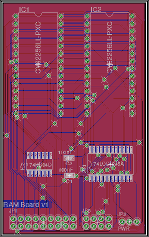
**UPDATE:** I have reworked the board due to major issues with the connectors and pin holes *(17 September 2014)*
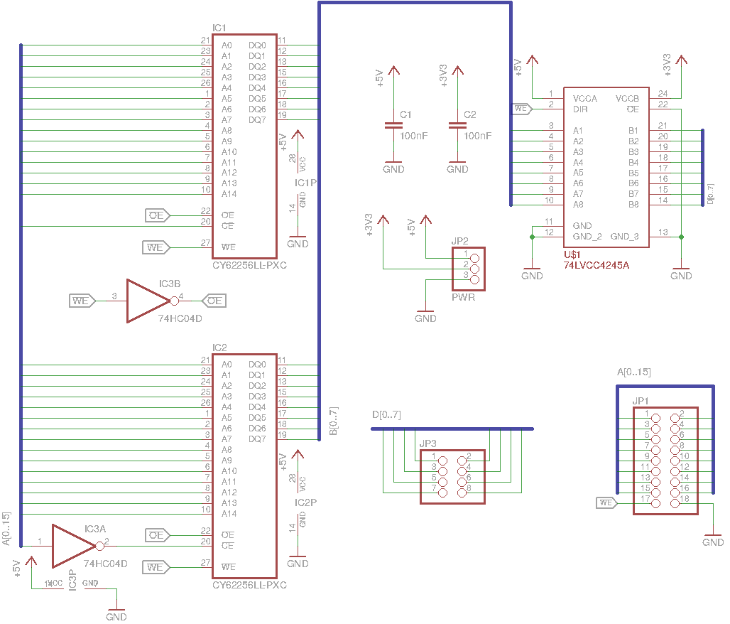
The CUPC/8 CPU has a 16-bit address bus and therefore a maximum addressable memory of 64KB (without bank switching, etc.).
The 64KB is provided by 2x 256Kbit SRAM chips (CY62256). Which chip is selected is determined by the MSB of the address line - addr(15). Chip select is simply driven directly off this line for the first chip and is passed through an inverter (NOT gate) to the second chip.
The Output Enabled logic is simply the inverse of the Write Enable signal so it too is passed through an inverter.
As the FPGA can only handle 3V3 inputs (and drive 3V3 outputs), and the SRAM chips are 5V, we use a bus transceiver on the data bus to provide logic level conversion. Level conversion isn't necessary on the address bus as the SRAM chips can happily work with 3V3 input logic (it's above the rated threshold).
The 16 address bus pins + write enable pin are connected to bank 2 of the FPGA (exhausting IO pins on that bank) and the data bus to bank 3.
BoM: